- 您现在的位置:买卖IC网 > Sheet目录3813 > PIC18F452-I/ML (Microchip Technology)IC MCU FLASH 16KX16 A/D 44QFN
PIC16C9XX
DS30444E - page 80
1997 Microchip Technology Inc.
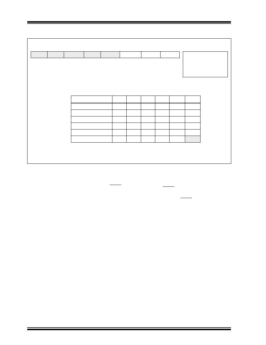
FIGURE 12-2: ADCON1 REGISTER (ADDRESS 9Fh)
U-0
R/W-0
—
PCFG2
PCFG1
PCFG0
R = Readable bit
W = Writable bit
U = Unimplemented
bit, read as ‘0’
- n = Value at POR reset
bit7
bit0
bit 7-3:
Unimplemented: Read as '0'
bit 2-0:
PCFG2:PCFG0: A/D Port Conguration Control bits
A = Analog input
D = Digital I/O
PCFG2:PCFG0
RA0
RA1
RA2
RA5
RA3
VREF
000
A
AVDD
001
A
VREF
RA3
010
A
AVDD
011
A
VREF
RA3
100
A
D
A
AVDD
111
D
—
The ADRES register contains the result of the A/D con-
version. When the A/D conversion is complete, the
result is loaded into the ADRES register, the GO/DONE
bit (ADCON0<2>) is cleared, and A/D interrupt ag bit
ADIF is set. The block diagram of the A/D module is
shown in Figure 12-3.
After the A/D module has been congured as desired,
the selected channel must be acquired before the con-
version is started. The analog input channels must
have their corresponding TRIS bits selected as an
input. To determine acquisition time, see Section 12.1.
After this acquisition time has elapsed the A/D conver-
sion can be started. The following steps should be fol-
lowed for doing an A/D conversion:
1.
Congure the A/D module:
Congure analog pins / voltage reference /
and digital I/O (ADCON1)
Select A/D input channel (ADCON0)
Select A/D conversion clock (ADCON0)
Turn on A/D module (ADCON0)
2.
Congure A/D interrupt (if desired):
Clear ADIF bit
Set ADIE bit
Set GIE bit
3.
Wait the required acquisition time.
4.
Start conversion:
Set GO/DONE bit (ADCON0)
5.
Wait for A/D conversion to complete, by either:
Polling for the GO/DONE bit to be cleared
OR
Waiting for the A/D interrupt
6.
Read A/D Result register (ADRES), clear bit
ADIF if required.
7.
For next conversion, go to step 1 or step 2 as
required. The A/D conversion time per bit is
dened as TAD. A minimum wait of 2TAD is
required before next acquisition starts.
发布紧急采购,3分钟左右您将得到回复。
相关PDF资料
PIC18F452-I/PT
IC MCU FLASH 16KX16 EE 44TQFP
PIC18F6622-I/PT
IC PIC MCU FLASH 32KX16 64TQFP
201828-1
CONN JACKSCREW SHORT-SHORT FMALE
608489070001049
CONN CONTACT FOR 8483/8484 PLUGS
PIC18LF258-I/SO
IC MCU CAN FLASH 16K LP 28-SOIC
DSPIC33FJ256GP710-I/PT
IC DSPIC MCU/DSP 256K 100TQFP
9-1469373-9
CONN GUIDE MOD FEMALE R/A
PIC32MX460F256L-80V/PT
IC MCU 32BIT 256KB FLASH 100TQFP
相关代理商/技术参数
PIC18F452-I/P
功能描述:8位微控制器 -MCU 32KB 1536 RAM 34I/O RoHS:否 制造商:Silicon Labs 核心:8051 处理器系列:C8051F39x 数据总线宽度:8 bit 最大时钟频率:50 MHz 程序存储器大小:16 KB 数据 RAM 大小:1 KB 片上 ADC:Yes 工作电源电压:1.8 V to 3.6 V 工作温度范围:- 40 C to + 105 C 封装 / 箱体:QFN-20 安装风格:SMD/SMT
PIC18F452-I/P
制造商:Microchip Technology Inc 功能描述:IC 8BIT FLASH MCU 18F452 DIP40
PIC18F452-I/PG
功能描述:8位微控制器 -MCU 32KB 1536 RAM 34I/O RoHS:否 制造商:Silicon Labs 核心:8051 处理器系列:C8051F39x 数据总线宽度:8 bit 最大时钟频率:50 MHz 程序存储器大小:16 KB 数据 RAM 大小:1 KB 片上 ADC:Yes 工作电源电压:1.8 V to 3.6 V 工作温度范围:- 40 C to + 105 C 封装 / 箱体:QFN-20 安装风格:SMD/SMT
PIC18F452-I/PT
功能描述:8位微控制器 -MCU 32KB 1536 RAM 34I/O RoHS:否 制造商:Silicon Labs 核心:8051 处理器系列:C8051F39x 数据总线宽度:8 bit 最大时钟频率:50 MHz 程序存储器大小:16 KB 数据 RAM 大小:1 KB 片上 ADC:Yes 工作电源电压:1.8 V to 3.6 V 工作温度范围:- 40 C to + 105 C 封装 / 箱体:QFN-20 安装风格:SMD/SMT
PIC18F452-I/PT
制造商:Microchip Technology Inc 功能描述:8BIT FLASH MCU SMD 18F452 TQFP44
PIC18F452-I/PTC28
制造商:Microchip Technology Inc 功能描述:
PIC18F452-I/PTG
功能描述:8位微控制器 -MCU 32KB 1536 RAM 34I/O RoHS:否 制造商:Silicon Labs 核心:8051 处理器系列:C8051F39x 数据总线宽度:8 bit 最大时钟频率:50 MHz 程序存储器大小:16 KB 数据 RAM 大小:1 KB 片上 ADC:Yes 工作电源电压:1.8 V to 3.6 V 工作温度范围:- 40 C to + 105 C 封装 / 箱体:QFN-20 安装风格:SMD/SMT
PIC18F452IL
制造商:Microchip Technology Inc 功能描述: